 English
Electrical Analysis
Electrical Characterization
JCET provides an array of electrical characterization services and support throughout the design process. Our worldwide Package Characterization team provides support from design centers located in Singapore, Arizona, California, and South Korea. JCET also provides characterization support in the areas of (1) Thermal Analysis (2) Mechanical Analysis and (3) Moldflow Analysis.
Electrical Characterization
At JCET, we also understand the influence of package interconnects on the overall system level signal integrity and power integrity. When it comes to high-speed digital, radio frequency (RF) or mixed-signal integrated circuits (ICs), our customers are looking for optimum package performance that complements the robustness of their chip designs in an actual system environment. JCET delivers this by using best-in-class, high-end 3D field solvers to predict and optimize the wideband electrical performance of high-speed package designs. Such package performance data is subsequently used in system-level models that are solved in the time domain and/or frequency domain to gain a deeper understanding of the package’s influence on system performance.
Package Modeling and Co-Design
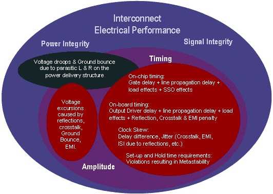
System level performance metrics such as reflections, crosstalk, propagation delay, skew, etc. on a signal path and those such as voltage dips and bounces on a power delivery path are key indicators of the acceptability of a package design. It is important to verify if the package’s electrical performance stays within the margins allowed in the system noise and timing budgets. S-parameter models of interconnects or single/multi-section lumped element equivalent circuits fitted to those S-parameters can be directly plugged into system models for an accurate prediction.
Signal Integrity and Power Integrity
System level performance metrics such as reflections, cross-talk, propagation delay, skew, etc. on a signal path and those such as voltage dips and bounces on a power delivery path are key indicators of the acceptability of a package design. It is important to verify if the package’s electrical performance stays within the margins allowed in the system noise and timing budgets. S-parameter models of interconnects or single/multi-section lumped element equivalent circuits fitted to those S-parameters can be directly plugged into system models for an accurate prediction.
JCET uses Ansoft Designer and Keysight ADS to perform end-to-end system simulations, in time domain and/or frequency domain, that can include device models from customers/vendors and circuit/behavioral models for interconnects. The timing and noise data output from such simulations enables our customers to make intelligent package design tradeoffs quickly throughout the package development cycle.
High Speed Electrical Design
Device operating frequencies in the GHz range or digital signals sub-ns edge rates make package interconnects electrically long in most traditional IC packages. Electrical performance prediction of such interconnect designs over a very wide band of frequencies, that encompasses the entire signal spectrum of interest, is critical for a successful design that fits with our “Right- First-Time” approach.
JCET uses and array or simulation tools to model even the most complex package design layouts with the desired levels of structural accuracy. Incorporating these full 3D electromagnetic field solvers and high-frequency simulators allows us to solve these structures accurately. We can then generate multi-port S-parameter behavioral models in the frequency domain, from DC through multiple tens of GHz that accurately display the output of the critical nets from a given substrate layout.