 English
Flip Chip packaging, in which the silicon die is directly attached to the substrate using solder bumps instead of wirebonds, provides a dense interconnect with the high electrical and thermal performance. Flip Chip interconnection provides the ultimate in miniaturization, reduced package parasitics and enables new paradigms in power and ground distribution to the chip not feasible in other traditional packaging approaches.
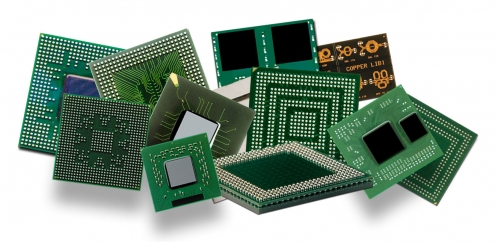
JCET offers a broad Flip Chip portfolio--from large single die packages with passive components to modules and complex advanced 3D packaging, with a variety of low cost and innovative options. JCET's extensive flip chip portfolio includes:
• FCBGA- singulated, exposed die package with capillary underfill (CUF)
• fcCSP - overmolded chip scale package with mold underfill (MUF) or CUF; available in ultra high density (UHD) and high density (HD) strip formats
• fcCSP-Hybrid - fcCSP variation that features a “hybrid” stacked construction, i.e., flip chip die on bottom and wirebond die on top
• fcLGA - exposed die product that uses "lands" instead of solder balls for second level interconnect
• fcCuBE – low cost, high performance advanced flip chip packaging technology
• Bare Die fcPoP - chip scale package with CUF
• Molded Laser fcPoP - molded laser chip scale package; also available in an exposed die configuration (PoP-MLP-ED)
• 3D TSV interconnect (Si-to-Si f-t-f / f-t-b bonding)
• FCOL-Flip Chip on Leadframe
Both FCBGA and fcCSP use solder balls for second level (BGA) interconnection.
A Transformative, Low Cost Flip Chip Solution: fcCuBE®
In addition, JCET offers innovative, low cost flip chip technology called "fcCuBE." fcCuBE is a low cost, high performance advanced flip chip packaging technology that features copper (Cu) pillar bumps, Bond-on-Lead (BOL) interconnection and other enhanced assembly processes. The name says it all: flip chip with Cu pillar, BOL and
Enhanced Processes.fcCuBE® technology is available across a wide range of platforms. Since receiving it first fcCuBE-related patent in 2006 on the innovative BOL process, JCET has invested heavily over the years in developing this transformative technology into a compelling filp chip solution a wide cross section of end products in the low to high end mobile market, as well as mid to high end consumer and cloud computing markets.
The advantages of fcCuBE are driving wide customer adoption form cost sensitive markets such as mobile and consumer to networking and cloud computing where increased routing density and performance are imperative. fcCuBE's unique BOL interconnect structure provides scalability to very fine bump pitches and high I/O while alleviating stress-related chip to package interaction (CPI), a common phenomenon associated with lead free and copper pillar bump structures. This is particularly important for mid-to high-end networking and consumer applications.
Full Turnkey Flip Chip Services at JCET
With our unmatched strength in wafer level packaging, wafer probe and final test, JCET is uniquely positioned to provide full turnkey processing to our customers. JCET offers full turnkey flip chip services ranging from design through production, including high speed, high pin count digital and RF testing.