
 English
MEMS and Sensors
With the growing consumer demand for smart devices capable of sensing, communicating and controlling applications, MEMS and Sensors are becoming a critical packaging approach due to their smaller footprint, thinner profile and functional integration capabilities. MEMS and sensors can be found in a wide range of systems in the communications, consumer, medical, industrial and automotive markets
Sensors
A sensor is a device or system that detects/measures a physical property and then records, reports and/or responds to the stimulation. Sensors are typically assembled in a module that responds based on the stimulation or feed to the sensor. There are many different types of sensors and applications such as:
• Pressure sensor
• Inertial sensor
• Microphone
• Proximity sensor
• Fingerprint sensor
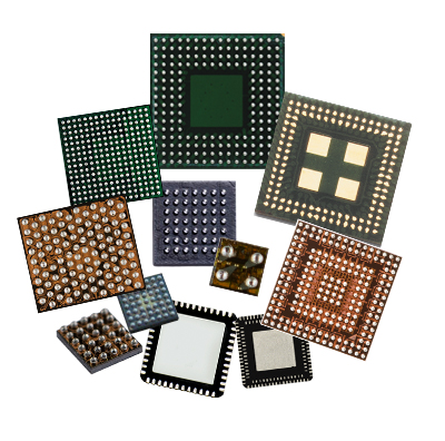
Micro-Electro-Mechanical-Systems (MEMS)
MEMS is a specialized sensor that combines mechanical and electrical components in a discrete format or a module. MEMS are typically multi-die solutions such as a sensing die paired with an application-specific integrated circuit (ASIC). A MEMS device can consist of mechanical elements, sensors, actuators, and electrical and electronics devices on a common silicon substrate. Some of the advantages of using a MEMS based sensor in consumer, automotive and mobile applications are smaller size, low power consumption, lower cost, etc.
Integrated Turnkey Solutions
Our broad technology portfolio and dedicated MEMS team can provide a comprehensive turnkey solution to support your production ramp, including package co-design, simulation, Bill of Material (BOM) qualification, assembly, quality assurance and in-house test solutions. JCET delivers smaller form factor, higher performance and lower cost solutions for our customers’ end products. Our innovative integration solutions can help your business achieve the size, performance and cost requirements for your MEMS and sensor applications.
1.embedded Wafer Level Ball Grid Array (eWLB) - single die, multi-die and stacked Package-on-Package configurations
2.Wafer Level Chip Scale Package (WLCSP) - very small single die
3.Flip Chip Chip Scale Package (fcCSP)- single or multi-die flip chip configurations
4.Fine Pitch Ball Grid Array (FBGA) - single or multi-die configurations
5.Land Grid Array(LGA) - single or multi-die configurations
6.Quad Flat No-Lead (QFN) - single or multi-die configurations
Full Turnkey Flip Chip Services at JCET
With our unmatched strength in wafer level packaging, wafer probe and final test, JCET is uniquely positioned to provide full turnkey processing to our customers. JCET offers full turnkey flip chip services ranging from design through production, including high speed, high pin count digital and RF testing.