


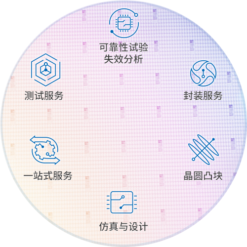


Wire bonding forms an interconnection between a chip to a substrate, substrate to substrate, or substrate to a package. Wire bonding is generally considered the most cost-effective and flexible interconnect technology, and is used to assemble the majority of semiconductor packages today.
Flip Chip packaging, in which the silicon die is directly attached to the substrate using solder bumps instead of wirebonds, provides a dense interconnect with high electrical and thermal performance. Flip Chip interconnection provides the ultimate in miniaturization, reduced package parasitics and enables new paradigms in power and ground distribution to the chip not feasible in other traditional packaging approaches.
Wafer bumping technology can provide significant performance, form factor and cost advantages in a semiconductor package.
Today’s consumers are looking for powerful, multi-functional electronic devices with unprecedented performance and speed, yet small, thin, and low cost. This creates complex technology and manufacturing challenges for semiconductor companies as they look for new ways to achieve greater performance and functionality in a small, thin, low cost device.
Demands for greater system performance, increased functionality, reduced power consumption, and reduced form factor require an advanced packaging approach known as system integration.
System integration is combining multiple integrated circuits (ICs) and components into a single system or modularized sub-system in order to achieve higher performance, functionality, and processing speeds with a significant reduction in space requirements inside the electronics device.
With the growing consumer demand for smart devices capable of sensing, communicating, and controlling applications, MEMS and Sensors are becoming a critical packaging approach due to their smaller footprint, thinner profile, and functional integration capabilities. MEMS and sensors can be found in a wide range of systems in the communications, consumer, medical, industrial, and automotive markets.
In power and analog device manufacturing, JCET leverages extensive expertise in wafer processing, advanced architectures, and high-temperature/thermal-diffusion materials.
While building world-class advanced packaging technology and large-scale production, JCET continually refines mainstream packaging—innovative process control and collaborative design boost reliability, cut costs, and expand applications.